
close
Choose Your Site
Global
Social Media


Views: 0 Author: Site Editor Publish Time: 2026-08-25 Origin: Site


For semiconductor and solar equipment manufacturers, integrating a new carrier system is a high-stakes decision. Material failure directly translates to severe yield loss, catastrophic particle contamination, or expensive automation crashes. You need consumable components you can trust implicitly. Polyvinylidene Fluoride (PVDF) remains an industry standard. It delivers an excellent balance of extreme chemical purity, robust chemical resistance, and high mechanical strength. However, qualifying a specific PVDF wafer carrier demands rigorous engineering validation. You must meticulously map the carrier dimensions against Equipment Front End Module (EFEM) tolerances. You must also account for process-specific thermal and chemical realities on the factory floor.
This guide outlines standard engineering frameworks, precise testing protocols, and intelligent vendor evaluation logic. We will show you exactly how to qualify these critical carriers for high-volume production environments. You will learn actionable steps to ensure seamless automation and flawless process integration.
Equipment makers face a tough balancing act constantly. They must deliver long-term durability and extreme chemical purity. Consumable components demand meticulous material selection. These specific parts go into wet benches, aggressive cleaning stations, and automated transport modules. Engineers often debate polymer choices heavily. Why choose PVDF over other advanced polymers?
Compared to PFA or PTFE, PVDF offers vastly superior mechanical strength. You get excellent dimensional stability immediately. Carriers show much less warping under heavy silicon loads. Precision robotic handling relies entirely on this structural rigidity. PTFE tends to creep slowly under continuous stress. PVDF maintains its shape reliably over time. You avoid sudden robotic handler drops.
Compared to PEEK, PVDF delivers a highly effective solution. It works perfectly for mid-temperature ranges up to roughly 150°C. It handles aggressive wet chemistry environments exceptionally well. Hydrofluoric (HF) acid and concentrated nitric acid baths degrade many standard plastics. PVDF withstands these harsh chemicals effortlessly. PEEK might offer slightly higher temperature resistance, but it costs significantly more. PVDF strikes the perfect economic and technical balance.
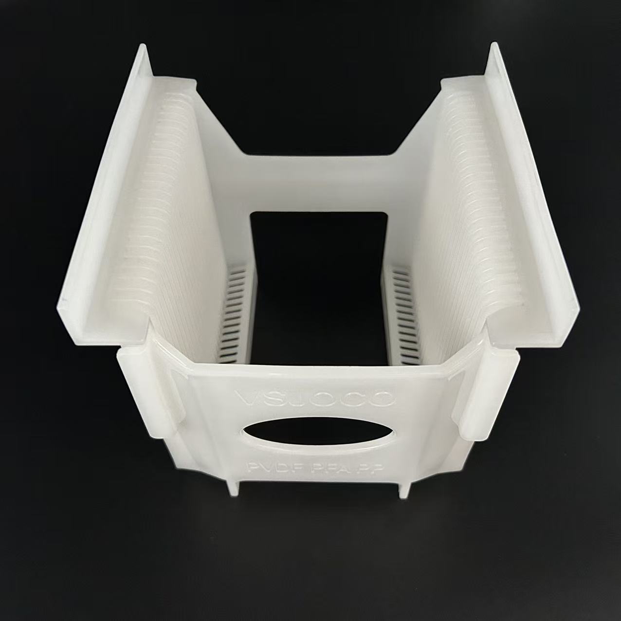
A successful qualification proves something crucial. The semiconductor wafer basket extends component lifespan drastically. It also reduces defect density across the manufacturing line. You achieve better overall equipment effectiveness directly. You maximize yield rates consistently. We must ensure every carrier meets exact engineering specifications.
Polymer Performance Profile
| Material | Mechanical Rigidity | Chemical Resistance (Acids) | Max Operating Temp |
|---|---|---|---|
| PTFE / PFA | Low (Prone to creep) | Extreme | ~260°C |
| PEEK | Very High | Moderate (Weak to HF) | ~250°C |
| PVDF | High | Excellent | ~150°C |
You must verify pitch precision and pocket design meticulously. Overall warpage limits need strict evaluation under full load. This ensures seamless compatibility. Standard EFEM end-effectors require exact spatial alignment. Any sub-millimeter deviation leads to dropped wafers. Automation crashes halt production lines instantly. You lose thousands of dollars per minute during downtime.
Map all carrier dimensions against relevant SEMI specifications directly. FOUP or FOSB interfaces demand precise geometry. You might use the carrier as an inner cassette frequently. Compliance prevents physical transport jams. Always double-check standard interface guidelines before starting pilot tests.
Common mistakes happen during initial robotic teaching. Engineers sometimes ignore micro-misalignments. These tiny spatial errors amplify dramatically at full operational speeds. Always calibrate end-effectors using fully loaded carriers. Dynamic weight changes structural deflection significantly.
Develop strict protocols to analyze trace metal contamination. Look closely at parts-per-billion (ppb) or parts-per-trillion (ppt) levels. The PVDF wafer cassette faces proprietary cleaning chemistries constantly. Purity remains absolutely non-negotiable. Even minute metallic leaching destroys semiconductor device yields completely.
Evaluate volatile organic compound (VOC) emissions carefully. Test them under hard vacuum states. Test them at elevated temperatures repeatedly. This guarantees lens and process chamber integrity. Adjacent process steps rely heavily on a pristine environment. Outgassing leaves destructive residues on critical optical components.
Best practices include continuous static soak tests. Submerge carriers in process chemicals for extended periods. Analyze the bath fluid afterward. Use Inductively Coupled Plasma Mass Spectrometry (ICP-MS) for this step. This reveals hidden extractables clearly. It prevents contamination surprises during high-volume manufacturing.
Identify the exact point of physical dimensional distortion. Test this boundary during repeated, aggressive heating cycles. Cool the carriers rapidly to simulate process thermal shock scenarios. You need to know exactly when structural fatigue begins. Polymers expand and contract continuously. You must map this thermal behavior accurately.
Assess particle generation rigorously. Wafers get inserted and extracted repeatedly. High-throughput operations cause continuous friction. You must monitor any micro-abrasions closely. Shedding particles ruin delicate circuitry instantly. Use liquid particle counters (LPC) in deionized water baths. This quantifies mechanical wear accurately. It helps establish preventative maintenance schedules.
Evaluate carbon-filled or specialized ESD-safe formulations thoroughly. Static discharge poses massive risks. Sensitive compound semiconductors suffer catastrophic damage easily. Ultra-thin films degrade rapidly under minor electrostatic shocks. You must bleed off static charges safely during fast spin-rinse drying cycles. Triboelectric charging happens whenever water moves rapidly across polymer surfaces.
Balance the addition of conductive fillers intelligently. These additives can sometimes compromise chemical purity. Carbon nanotubes or carbon black provide excellent electrical conductivity. However, they might leach into aggressive acid baths over time. You must find the optimal middle ground. Test surface resistivity thoroughly across the entire carrier body.
Static Dissipation Range Chart
| Material Type | Surface Resistivity (Ohms/sq) | Application Suitability |
|---|---|---|
| Virgin PVDF | > 10^14 | High Purity Wet Process |
| ESD-Safe PVDF | 10^6 - 10^9 | Dry Transport / Sensitive Films |
| Conductive PVDF | < 10^5 | High Static Environments |
Test the wafer transport carrier thoroughly across different substrates. It needs to securely hold ultra-thin wafers. Bowed substrates present unique physical handling challenges. Assess varying diameters for silicon carbide (SiC) or gallium nitride (GaN) applications. Ensure no edge chipping occurs during fast automated insertions. Pocket draft angles must accommodate different edge profiles perfectly.
Laboratory tests provide a solid baseline. However, factory floors introduce unpredictable process variables. You must follow a structured implementation sequence. This mitigates operational risks effectively. We highly recommend a strict three-phase validation approach.
Acknowledge reality openly. Standard laboratory tests rarely replicate exact hydrodynamic forces. Fluid dynamics inside a specific wet bench vary wildly. Laminar flow behaves differently than turbulent flow around carrier pockets. Field pilot data is simply non-negotiable. You must validate performance in the actual process tool.
We highly recommend setting up a dedicated pilot cell. Run test wafers through the exact chemical sequence. Monitor particle adders on the wafers meticulously. Inspect the carrier pockets for discoloration or swelling. These physical signs indicate impending material failure. Act proactively based on pilot data. Do not wait for a full production lot to fail.
Require strict documentation of virgin PVDF resin sourcing. This prevents batch-to-batch purity inconsistencies. A high-purity wafer carrier demands pristine raw materials. Regrind or recycled polymers introduce unacceptable contamination risks. Ask vendors for certificates of analysis (COA) for every single batch. Track these documents diligently.
Evaluate vendor injection molding capabilities closely. Verify whether molding and packaging occur inside certified ISO cleanrooms. Exposure to airborne particulates during manufacturing ruins the carrier. Airborne molecular contamination (AMC) is a serious, invisible threat. Cleanroom molding ensures baseline cleanliness from day one. You should audit their facility personally.
Determine vendor engineering agility. Can they modify carrier pitch? Can they adjust pocket draft angles quickly? Proprietary equipment geometries often demand bespoke physical adjustments. Off-the-shelf solutions rarely fit perfectly. A flexible vendor accelerates your time to market. They adapt to your engineering revisions swiftly.
Take clear next-step actions now. Request material safety data sheets (MSDS) immediately. Ask for comprehensive trace metal analysis reports. Procure sample units for initial EFEM fit-checks. Test these samples extensively before signing bulk procurement contracts. Vendor transparency builds long-term manufacturing trust.
A: Typically, virgin PVDF maintains structural integrity up to 140°C–150°C, but dynamic loads at these temperatures require empirical testing to ensure dimensional stability.
A: Standard practice involves liquid particle counting (LPC) in DI water baths after mechanical abrasion tests, simulating the friction of robotic end-effectors.
A: Yes, but the qualification criteria differ. Solar applications often prioritize throughput and aggressive etching resistance, while advanced semiconductor nodes require extreme scrutiny on trace metal purity and sub-micron particle generation.
A: Depending on the complexity of the process (e.g., simple transport vs. active wet chemical processing), qualification usually spans 3 to 6 months, encompassing static measurement, dynamic cycling, and process environment pilot runs.


